(734) 344-4295
The physical product of the electronics engineer
While the schematic is designed to be easily readable by a human, the PCB is designed to be functional.
A PCB might have hundreds of individual copper traces - each of which are carefully thought-out and planned by the designer. The placement of some are more critical than others, but none are carelessly placed. Even though there are software packages available to "auto-route" a PCB (which is the process of automatically placing all traces on the circuit board), they are generally used only by the novice. Factors such as electromagenetic interference, electrostatic discharge, cross-talk, and others are not considered by an auto-router. An intelligent, artistic individual is required to ensure proper placement of every part of the circuit board. That is why some call it PCB Artwork instead of just PCB Design. PCB Design is an art form.
In some cases, such as high frequency or in sensitive circuitry, the circuit will not function at all unless properly laid out on the PCB.
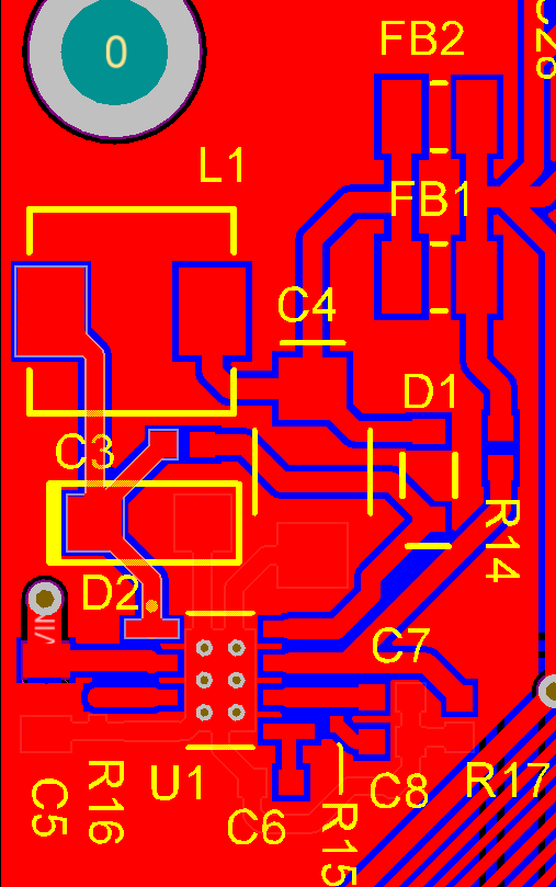
This example shows the same 5 Volt regulator that is shown on the Schematic Design Page.
In this example, placement is critical due to the high frequency voltage switching in the regulator circuit. Notice how some of the parts are placed closely together. This lowers the parasitic loop inducatnce in the high frequency current path, and is essential for proper operation of this circuit.
The physical 3D bodies shown in the image are the actual parts that the schematic symbolically represents.
The 2D Design File |
The 3D Design File |
|

|


